-
-
Written by Sherneyko Plata Rangel
-
Category: PYNQ-Z2
-
-
Hits: 18373
Written by Sherneyko Plata Rangel
Pynq-z2: Hello world
In this tutorial we will implement a simple test of the inputs/outputs available on our board, in order to familiarize with it and test that we can program it without any issues.
- First we will start a project from scratch, on Vivado, in this case we will use Vivado 2019.1, some options may vary depending on the version you are using:

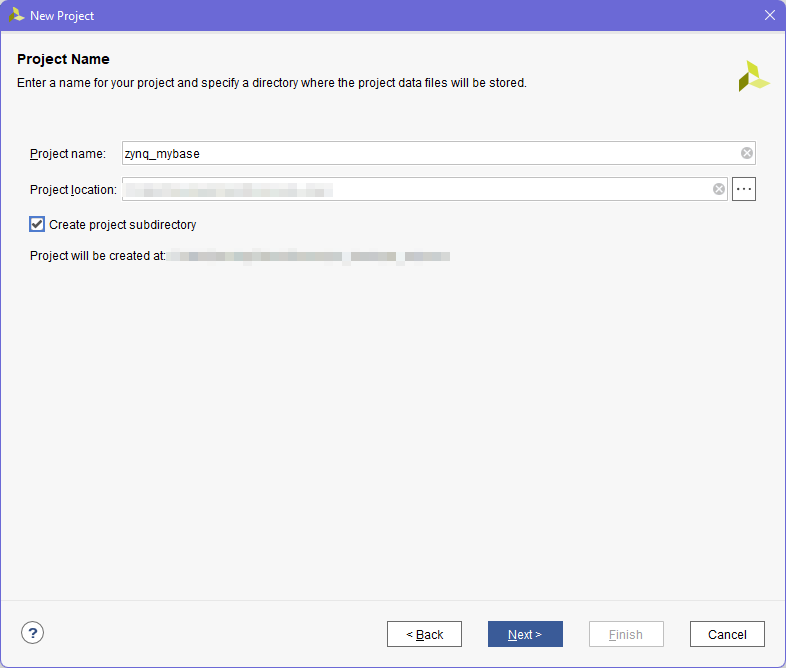
- Then we will name our project, and its path.
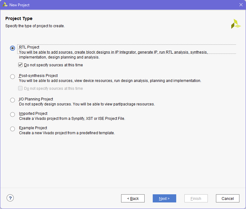
- We will create an empty RTL project. We will specify sources later.
- Select the FPGA part to work with. For pynq-z2, the part name is XC7z020clk400-1.

- Finally, press finish. An empty project for the selected part will be created in the path we specified before. Vivado automatically creates a directory hierarchy for our project. Since we dont need to explore it yet, we will extract
 zynq_mybase_src.zip into the projects directory

- For sake of simplicity, we will use ./v and ./xdc folders for our verilog sources and constraint files, respectively. Then, on vivado, we will add our sources to the project(
 zynq_mybase_src.zip).
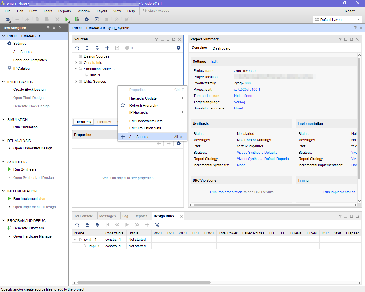
- Select add or create constraints, click next, then click on the “+” , and navigate to the xdc folder we extracted before. Select “io.xdc” and click ok


- Now, lets add our verilog sources. Select add or create design sources, click next, then click on the “+” , and navigate to the v folder we extracted before. Select “top.v” and click ok

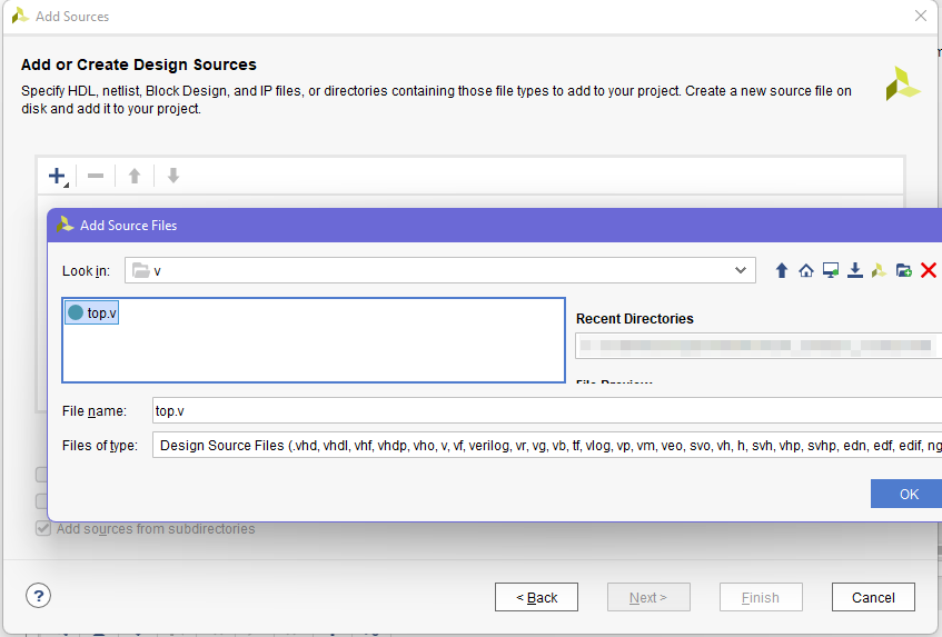
- Our project has now a top module, and a constraint file. We will now review these files

 |
Top.v
Module and inputs/outputs declaration
Port names on our top module must match names in our io.xdc
Internal wires for connecting test modules to some of our IOs
Clocking wizard. Will take an onboard clk of 125MHz (sysclk), and generate our design clk. This is a xilinx IP core, so we will have to create an instance of it first.
Virtuail IO. Will allow us to capture and generate signals from vivado. This is a xilinx IP core, so we will have to create an instance of it as well
Assignment of onboard buttons, switches to VIO inputs
Assignment of VIO outputs to onboard LEDs
|
 |
io.xdc
PACKAGE_PIN <pin>
specifies a pin on the FPGA
IOSTANDARD <iostandard> specifies the voltage level of the pin
get_ports <name>
specifies a port from the top level (top.v) to connect to
Basically each line maps a port to a FPGA pin, and specifies its IO type.
Note that port arrays need to be mapped one by one
|
- Lets create our Clocking wizard, VIO instances. Open the IP Catalog, and search for clocking wizard

- Set the input clock to 125M
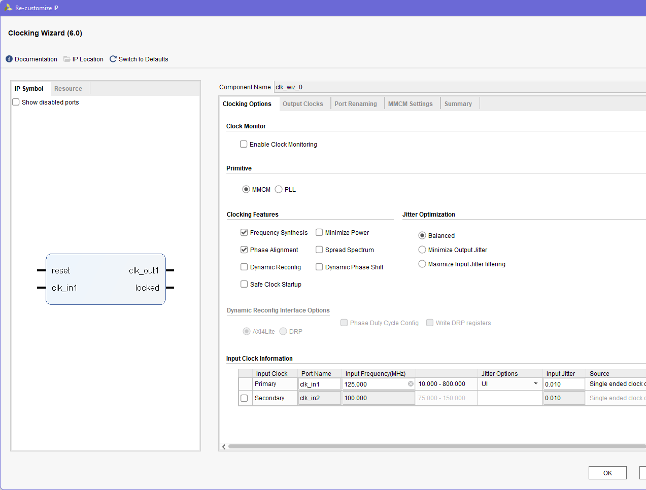
- And the output clock to 100M

- Then click OK to generate it. You can choose to generate the output product now, or skip it (will be done anyways when compiling the top module)
- Now lets repeat the process for our VIO, We will use 1 input probe and 1 output probe, both of 16 bits.

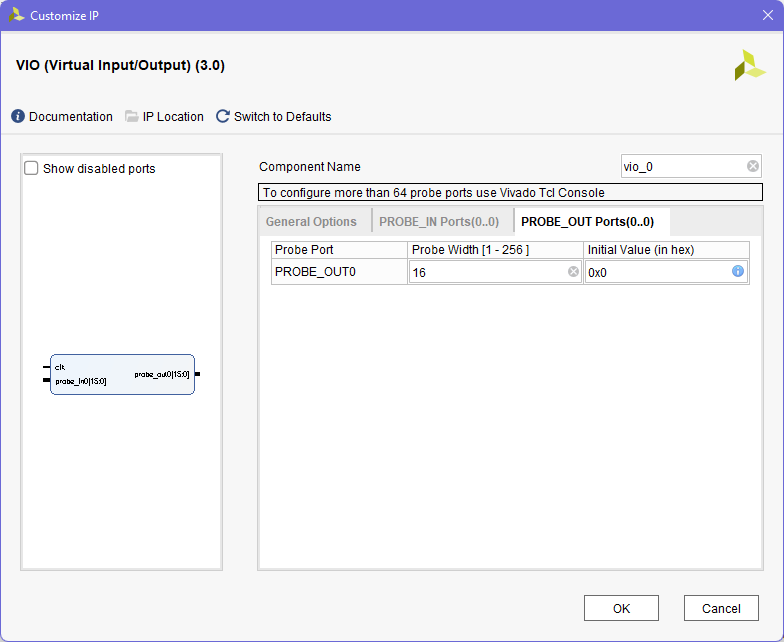
- Now that our project seems to have no missing sources, we can try to compile it.
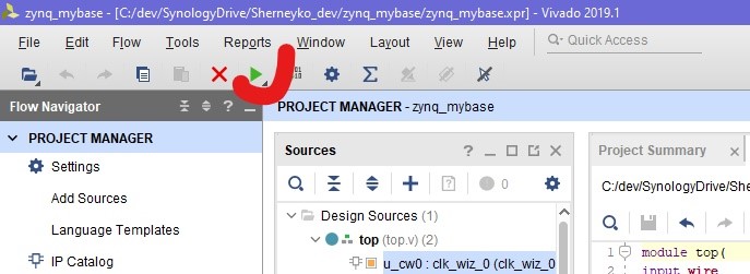
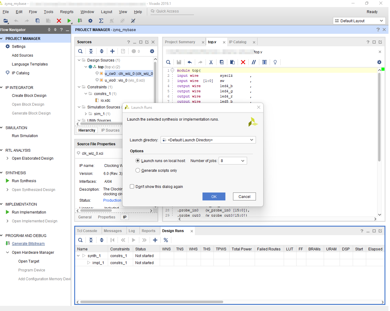
- After compilation is finished, its possible to download the design to the pynq-z2.
- With the board connected to our PC via USB, and powered on, click on Prorgram and debug > Open hardware manager > Open target

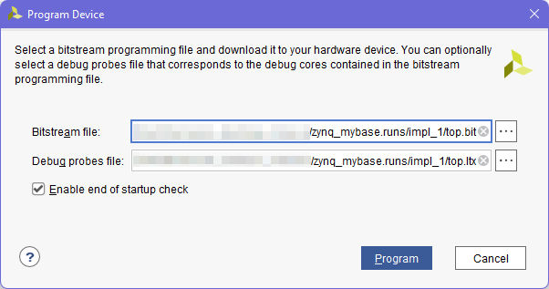
- Then click program device, and select xc7020_1.

- On the program device pop-up, you can select the bitsream and debug probes file. Most times it will automatically load the last compiled bitfile, with its matching debug probes file. Probes file needs to match the debugging logic in the bitfile being downloaded, otherwise it wont be able to connect. If any part of the debugging logic has a design error (missing connections, unmet timing), the debug probes file might not be generated, and it would not be possible to access debugging logic this way.
- Go to the hw_vio_1 and add all ports.

- Set all output ports bits o be controlled as toggle buttons
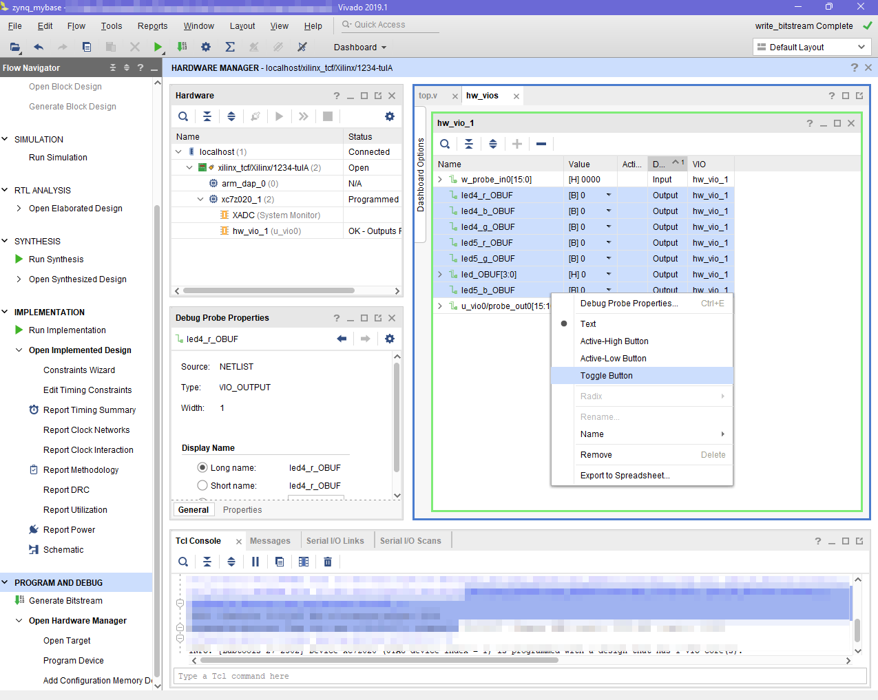
- Finally, test pressing some buttons/switches onboard, and see how the input probes change Also toggle some buttons on the VIO to control the onboard leds.

Enjoy!