-
-
Written by Holguer Becerra
-
Category: Cores
-
-
Hits: 10987
Written by Holguer Andres
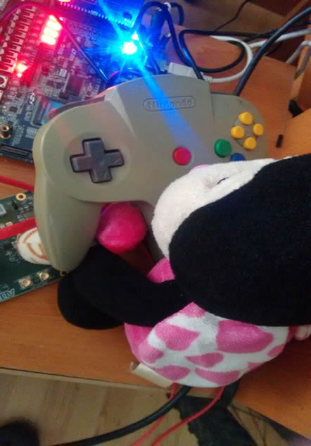
In this manual you are going to understand how the N64 Controller works, and how we can acquire through a simple Finite State Machine (FSM), all the buttons states from the N64 controller using the DE0-NANO (you can use any FPGA board, and implement this manual).
it is important to make clear that this manual is based on http://larsivar.com/wp/?p=86 manual in which it is explained the N64 controller protocol, there is a software example for acquiring the buttons states. However in this example, the given AVR driver is ported to a simple Verilog Module, which can be simply instantiated as many times as the user desire without affecting any performance, taking advantage of the FPGA parallelism.
Required Materials:
- Any FPGA board (Though for this manual we are going to use the DE0-NANO).
- N64 Controller(18 CADs on Amazon).
Brief Explanation:
- Let's start by looking at the N64 contoller Pinout:
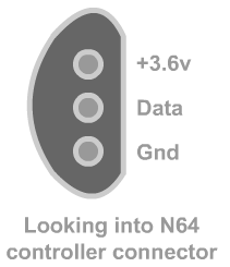
As you can see on the image, the N64 controller interface has only 3 pins of which only one(Data) is used to drive the controller.
- Now let's try to understand how we can obtain the n64 buttons states through the Data pin. The first thing we should know it is that this pin behaves as a bidirectional pin, and the N64 plays the roll of a slave that we must command with a Master Module, therefore we are going to drive the controller through a Master module that will be in charge of sending data to the controller, and vise versa. To have a better panorama about this scheme, you can take a look at the following image.
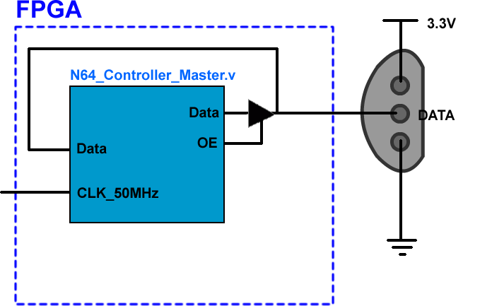
- It is important to know that for getting the states of the N64 buttons, the Master module must send 9 bits. The first bit corresponds to a starting flag (Wakes up indicating that a command will be sent), and the next 8 bits correspond to a command(which tells the controller what data we are inquiring). Then after we send the first 9 bits through the DATA signal, the controller will answer with 34 bits.

- Therefore, while the first nine bits are being sent the OE must be set to '1' to tell the bidirectional buffer and the controller we are sending data, and once these 9 bits are sent, the N64 will send the 34 bits as answer, hence, the OE shall be connected to '0' in order to capture the incoming data.
- Timing is very important to talk to the N64 Controller, otherwise the controller is not going respond properly according to the already mentioned description. Thus, there are timing control we must have at the moment of sending the output signal (Zero flag and the 8 bits). Furthermore, the Verilog Module was designed to work at 50MHz, which it is vital to take into account when designing the FSM to generate the control signal.
- There are two kind of signals we can send to the controller through the FSM, or we can receive from the N64 controller, these signal can be either 'Zero' or 'One'
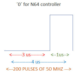
- Sending a '0':
- Sending a '1':
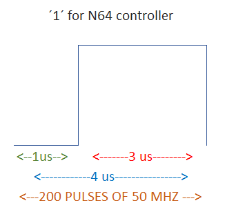
- As it could be observed on the previous images, for sending '0' the low signal remains longer (3us) whereas for sending '1' the lower signal remains just 1us.
- Now it is time to put into words, and detail the behaviour of the first nine bits that have to be sent to the controller.
- Initially the OE is assumed to be connected to '0'.
- Then the OE is set to '1'.
- Then the first bit or the flag has to be sent, this flag corresponds to a Zero.
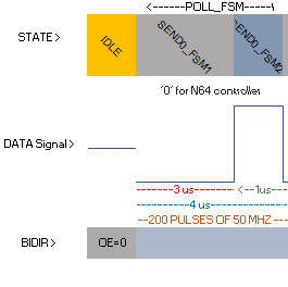
- Now the next 8 bits have to be sent, and the command to tell the controller ''Hey give me the buttons states!!" is 8'b00000011, as you can see in the following signal representation.

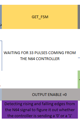
- Once the the 9 bits have been sent, the FSM has to wait until the N64 controller has replied with 34 bits (in this case we are only interested in the first 33 bits, so we can get rid of the 34th bit, which only contains the stop bit)
- After the N64 controller has sent the pulses indicating the different states of the buttons, the FSM has to wait for 100ms to give time to the controller, subsequently to send a finish signal.
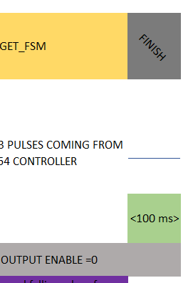
- Here the complete signal specs.
- Once the logical procedure is understood, the following step is to put this into a FSM Diagram to make it more understandable.
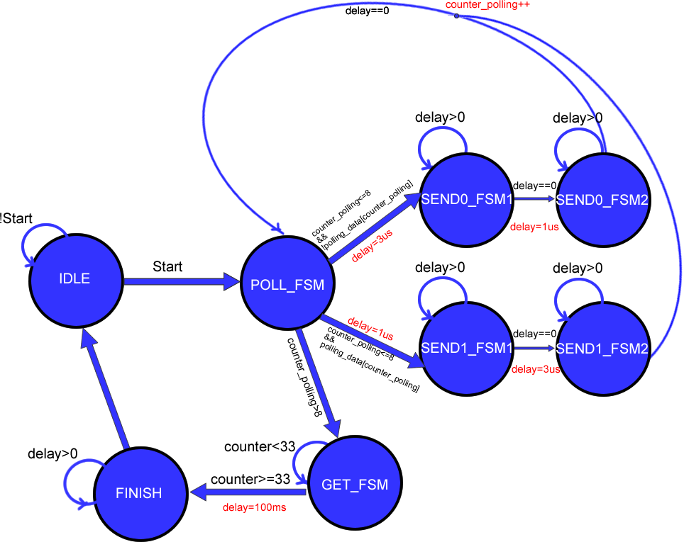
The previous FSM diagram is composed by 8 different states which are necessary to generate the control signal('9 bits'), and to wait for the N64 response.
- IDLE: In this state the FSM only goes to the "POLL_STATE", and polling_data is set to zero when a start signal is given, this start signal is simply an input pin described in Verilog.
- POLL_FSM: In this state the FSM has three different branches
- if counter_polling is less or equal to 8 and the polling_data[counter_polling ] is zero, the states goes to SEND0_FSM1, and a delay counter is set to 3us.
- if counter_polling is less or equal to 8 and the polling_data[counter_polling ] is one, the states goes to SEND1_FSM1, and a delay counter is set to 1us.
- if counter_polling is greater than 8, the states goes to GET_FSM.
It is important to know that the "polling_data" is just a bus of 9 bits connected to 9'b110000000, and the counter_polling is set to zero by the IDLE state. So if the polling_data is 0 the signal is going to be sent to the controller is a 0, which corresponds to maintain the output set to 0 for 3 us and then 1us to 1.
- SEND0_FSM1: in this state, there is countdown of the register "delay" which corresponds to the number of pulses of 50 MHz required to wait for 3 us (150 pulses), once the register reaches 0, the state goes to the next State SEND0_FSM2.
- SEND1_FSM1: in this state, there is countdown of the register "delay" which corresponds to the number of pulses of 50 MHz required to wait for 1 us(50 pulses), once the register reaches 0, the state goes to the next State SEND1_FSM2.
- SEND0_FSM2, and SEND1_FSM2: Same as their predecessors, then go back to "POLL_FSM", the delay counter is set to 400000 pulses or 100 ms.
- GET_FSM: In this state the FSM waits until an external logic to the FSM counts the number of falling pulses and rising pulses (sync), determines whether the incoming signal is '0' or '1', and stores the captured signal into a shift register.
- FINISH: in this state, there is a countdown of the register delay, once the register reaches 0, the state goes to IDLE.
- Now it is time to see the Verilog Code, for this logic.
- Verilog Module pinout:
module N64_controller(
		input clk_50MHZ,
		inout data,
		input start,
		output reg [33:0]buttons=34'd0,
		output reg alive=1'd0
);
- States and control signals declaration:
								  //counter_en___finish___oe__get__state
localparam IDLE_FSM		 =	8'b0___________0________0___0_0000;
localparam POLL_FSM		 =	8'b0___________0________1___0_0000;
localparam SEND0_FSM1	 =	8'b0___________0________1___0_0010;
localparam SEND0_FSM2	 =	8'b0___________0________1___0_0011;
localparam SEND1_FSM1	 =	8'b0___________0________1___0_0100;
localparam SEND1_FSM2	 =	8'b0___________0________1___0_0101;
localparam GET_FSM 		 =	8'b1___________0________0___0_0110;
localparam FINISH_FSM 	 =	8'b0___________1________0___0_1110;


localparam THREEuSECONDS = 32'd150;
localparam ONEuSECONDS = 32'd50;
localparam HUNDRED_MS = 32'd400000;

reg [7:0]state=IDLE_FSM;
reg [31:0]counter_delay =32'd0;
reg [31:0]counter_delay_pulses =32'd0;
reg [3:0]counter_polling =4'd0;
reg [5:0]counting_data =6'd0;
wire [8:0]polling_data=9'b110000000;
reg [33:0]buffer_buttons=34'd0;
reg [7:0]counter=8'd0;
wire counter_en=state[7];
wire oe=state[5];
wire finish=state[6];
wire counting_data_clk=state[4];
wire data_out=state[0];
reg data_in=1'b0;
reg real_in=1'b0;
reg start_counter=1'b0;
assign data = oe ? data_out: 1'bz;
- Main FSM:
always@(posedge clk_50MHZ)
begin
	case(state[7:0])
	IDLE_FSM	:begin
					counter_delay[31:0]<=0;
					state[7:0]<=IDLE_FSM;
					if(start)
					begin
						state[7:0]<=POLL_FSM;
					end
				 end
	POLL_FSM	:begin
					counter_delay[31:0]<=0;// otherwise go to get the data
					state[7:0]<=GET_FSM;
					if(counter_polling[3:0]<=4'd8)
					begin
						counter_delay[31:0]<=ONEuSECONDS;//send a 1 starting from 1 us
						state[7:0]<=SEND1_FSM1;
						if(polling_data[counter_polling[3:0]]==1'b0)
						begin
							counter_delay[31:0]<=THREEuSECONDS;
							state[7:0]<=SEND0_FSM1;//send a 0  starting from 3 us
						end
					end
				 end
	SEND0_FSM1	:begin// send a 0
					state[7:0]<=SEND0_FSM1;
					counter_delay[31:0]<=counter_delay[31:0]-1'b1;
					if(counter_delay[31:0]==32'd0)
					begin
						state[7:0]<=SEND0_FSM2;
						counter_delay[31:0]<=ONEuSECONDS;
					end
				 end
	SEND0_FSM2	:begin
					state[7:0]<=SEND0_FSM2;
					counter_delay[31:0]<=counter_delay[31:0]-1'b1;
					if(counter_delay[31:0]==32'd0)
					begin
						state[7:0]<=POLL_FSM;
					end
				 end
	SEND1_FSM1	:begin
					state[7:0]<=SEND1_FSM1;
					counter_delay[31:0]<=counter_delay[31:0]-1'b1;
					if(counter_delay[31:0]==32'd0)
					begin
						state[7:0]<=SEND1_FSM2;
						counter_delay[31:0]<=THREEuSECONDS;
					end
				 end
	SEND1_FSM2	:begin
					state[7:0]<=SEND1_FSM2;
					counter_delay[31:0]<=counter_delay[31:0]-1'b1;
					if(counter_delay[31:0]==32'd0)
					begin
						state[7:0]<=POLL_FSM;
					end
				 end
	GET_FSM 	:begin
					state[7:0]<=GET_FSM;
					counter_delay[31:0]<=HUNDRED_MS;// DELAY AFTER POLLING AND GETTING DATA
				   if(counter[7:0]>=8'd33)// wait untilt there are 33 pulses coming from the N64 controller
					begin
						state[7:0]<=FINISH_FSM;
					end
				 end
	FINISH_FSM 	:begin
					state[7:0]<=FINISH_FSM;
					counter_delay[31:0]<=counter_delay[31:0]-1'b1;
					if(counter_delay[31:0]==32'd0)
					begin
						state[7:0]<=IDLE_FSM;
					end
				 end
	default		:begin
					state[7:0]<=IDLE_FSM;
					counter_delay[31:0]<=32'd0;
				 end
	endcase
end
- Counting pulses GET_FSM state:
async_trap_and_reset async_trap_and_reset_inst
(
.async_sig(data_in) , // input async_sig_sig
.outclk(clk_50MHZ) , // input outclk_sig
.out_sync_sig(sync_data) , // output out_sync_sig_sig
.auto_reset(1'b1) , // input auto_reset_sig
.reset(1'b1) // input reset_sig
);
async_trap_and_reset async_trap_and_reset_inst2
(
.async_sig(~data_in) , // input async_sig_sig
.outclk(clk_50MHZ) , // input outclk_sig
.out_sync_sig(sync_data_not) , // output out_sync_sig_sig
.auto_reset(1'b1) , // input auto_reset_sig
.reset(1'b1) // input reset_sig
);
always@(posedge clk_50MHZ)
begin
if(sync_data)
begin
counter<=counter+1'b1;
end
else
begin
counter<=counter;
if(!counter_en)
begin
counter<=0;
end
end
end
- Counter counter_polling:
always@(posedge data_out, posedge finish)
begin
if(finish)
begin
counter_polling[3:0]<=4'd0;
end
else
begin
counter_polling[3:0]<=counter_polling[3:0]+1'b1;
end
end
- Determining the logic level of the incoming signal from the controller:
always@(posedge clk_50MHZ)
begin
counter_delay_pulses<=counter_delay_pulses;
if(sync_data_not)
begin
buttons[counter]<=(counter_delay_pulses[31:0]>=32'd100);
end
else if(sync_data)
begin
counter_delay_pulses<=0;
end
else
begin
if(counter_en)
begin
counter_delay_pulses<=counter_delay_pulses+1'b1;
end
end
end
- Once we have taken a look at the FSM diagram and the Verilog description, we can simulate using ModelSim to verify that the designed FSM works properly, and we meet the timing specifications.
(right click on the image and open into a new window to magnify)

- Finally, after designing and simulating, we are ready to implement the module using any FPGA board, for this example, the DE0-NANO is used to conduct the experiment.
- ENJOY!!