Written by Sherneyko Plata Rangel


Pynq-z2: Hello world


In this tutorial we will implement a simple test of the inputs/outputs available on our board, in order to familiarize with it and test that we can program it without any issues.


  1. First we will start a project from scratch, on Vivado, in this case we will use Vivado 2019.1, some options may vary depending on the version you are using:


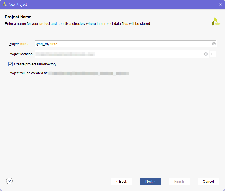
  2. Then we will name our project, and its path.


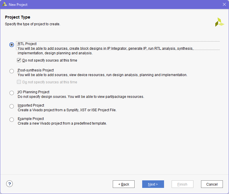
  3. We will create an empty RTL project. We will specify sources later.


  4. Select the FPGA part to work with. For pynq-z2, the part name is XC7z020clk400-1.


  5. Finally, press finish. An empty project for the selected part will be created in the path we specified before. Vivado automatically creates a directory hierarchy for our project. Since we dont need to explore it yet, we will extract Download this file (zynq_mybase_src.zip)zynq_mybase_src.zip into the projects directory


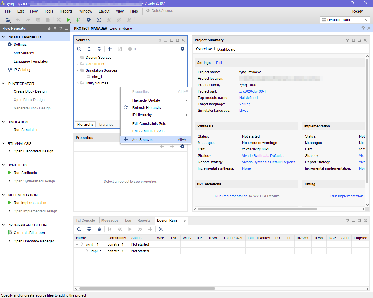
  6. For sake of simplicity, we will use ./v and ./xdc folders for our verilog sources and constraint files, respectively. Then, on vivado, we will add our sources to the project(Download this file (zynq_mybase_src.zip)zynq_mybase_src.zip).


  7. Select add or create constraints, click next, then click on the “+” , and navigate to the xdc folder we extracted before. Select “io.xdc” and click ok


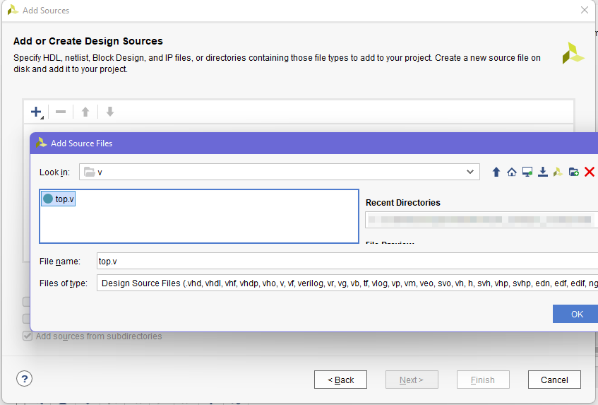
  8. Now, lets add our verilog sources. Select add or create design sources, click next, then click on the “+” , and navigate to the v folder we extracted before. Select “top.v” and click ok
    https://fpgalover.com/images/manuals/Pynq-z2/Vivado/intro/pynqz2_hworld_files/image013.png

    https://fpgalover.com/images/manuals/Pynq-z2/Vivado/intro/pynqz2_hworld_files/image013.png

  9. Our project has now a top module, and a constraint file. We will now review these files
    https://fpgalover.com/images/manuals/Pynq-z2/Vivado/intro/pynqz2_hworld_files/image013.png


     https://fpgalover.com/images/manuals/Pynq-z2/Vivado/intro/pynqz2_hworld_files/image013.png

    Top.v


    Module and inputs/outputs declaration


    Port names on our top module must match names in our io.xdc


    Internal wires for connecting test modules to some of our IOs


    Clocking wizard. Will take an onboard clk of 125MHz (sysclk), and generate our design clk. This is a xilinx IP core, so we will have to create an instance of it first.


    Virtuail IO. Will allow us to capture and generate signals from vivado. This is a xilinx IP core, so we will have to create an instance of it as well


    Assignment of onboard buttons, switches to VIO inputs


    Assignment of VIO outputs to onboard LEDs


     https://fpgalover.com/images/manuals/Pynq-z2/Vivado/intro/pynqz2_hworld_files/image013.png

    io.xdc


    PACKAGE_PIN <pin>
    specifies a pin on the FPGA


    IOSTANDARD <iostandard> specifies the voltage level of the pin


    get_ports <name>

    specifies a port from the top level (top.v) to connect to


    Basically each line maps a port to a FPGA pin, and specifies its IO type.


    Note that port arrays need to be mapped one by one

  10. Lets create our Clocking wizard, VIO instances. Open the IP Catalog, and search for clocking wizard
    https://fpgalover.com/images/manuals/Pynq-z2/Vivado/intro/pynqz2_hworld_files/image013.png

  11. Set the input clock to 125M
    https://fpgalover.com/images/manuals/Pynq-z2/Vivado/intro/pynqz2_hworld_files/image013.png

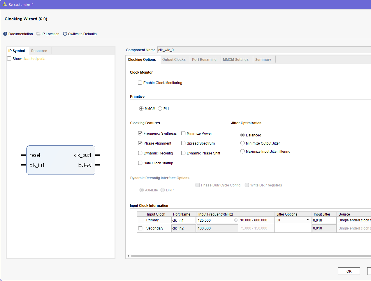
  12. And the output clock to 100M
    https://fpgalover.com/images/manuals/Pynq-z2/Vivado/intro/pynqz2_hworld_files/image013.png

  13. Then click OK to generate it. You can choose to generate the output product now, or skip it (will be done anyways when compiling the top module)

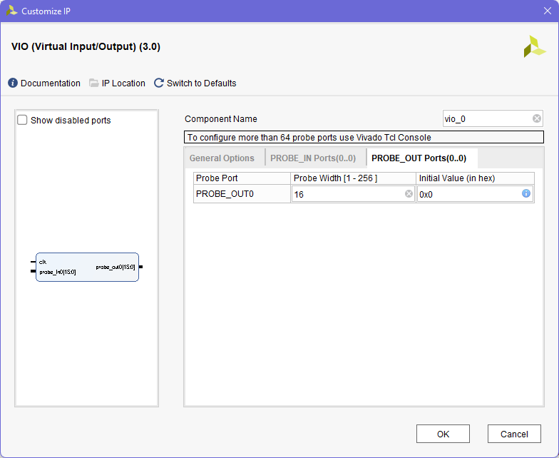
  14. Now lets repeat the process for our VIO, We will use 1 input probe and 1 output probe, both of 16 bits.
    https://fpgalover.com/images/manuals/Pynq-z2/Vivado/intro/pynqz2_hworld_files/image013.png
    https://fpgalover.com/images/manuals/Pynq-z2/Vivado/intro/pynqz2_hworld_files/image013.png

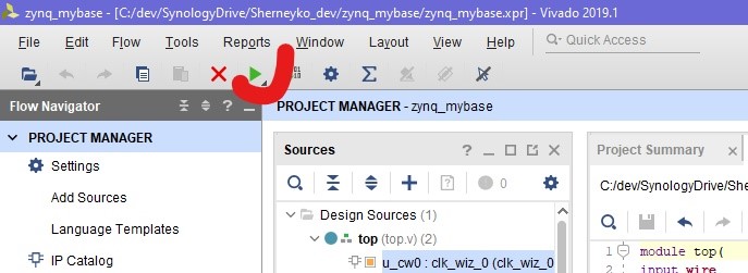
  15. Now that our project seems to have no missing sources, we can try to compile it.
    https://fpgalover.com/images/manuals/Pynq-z2/Vivado/intro/pynqz2_hworld_files/image013.png
    https://fpgalover.com/images/manuals/Pynq-z2/Vivado/intro/pynqz2_hworld_files/image013.png

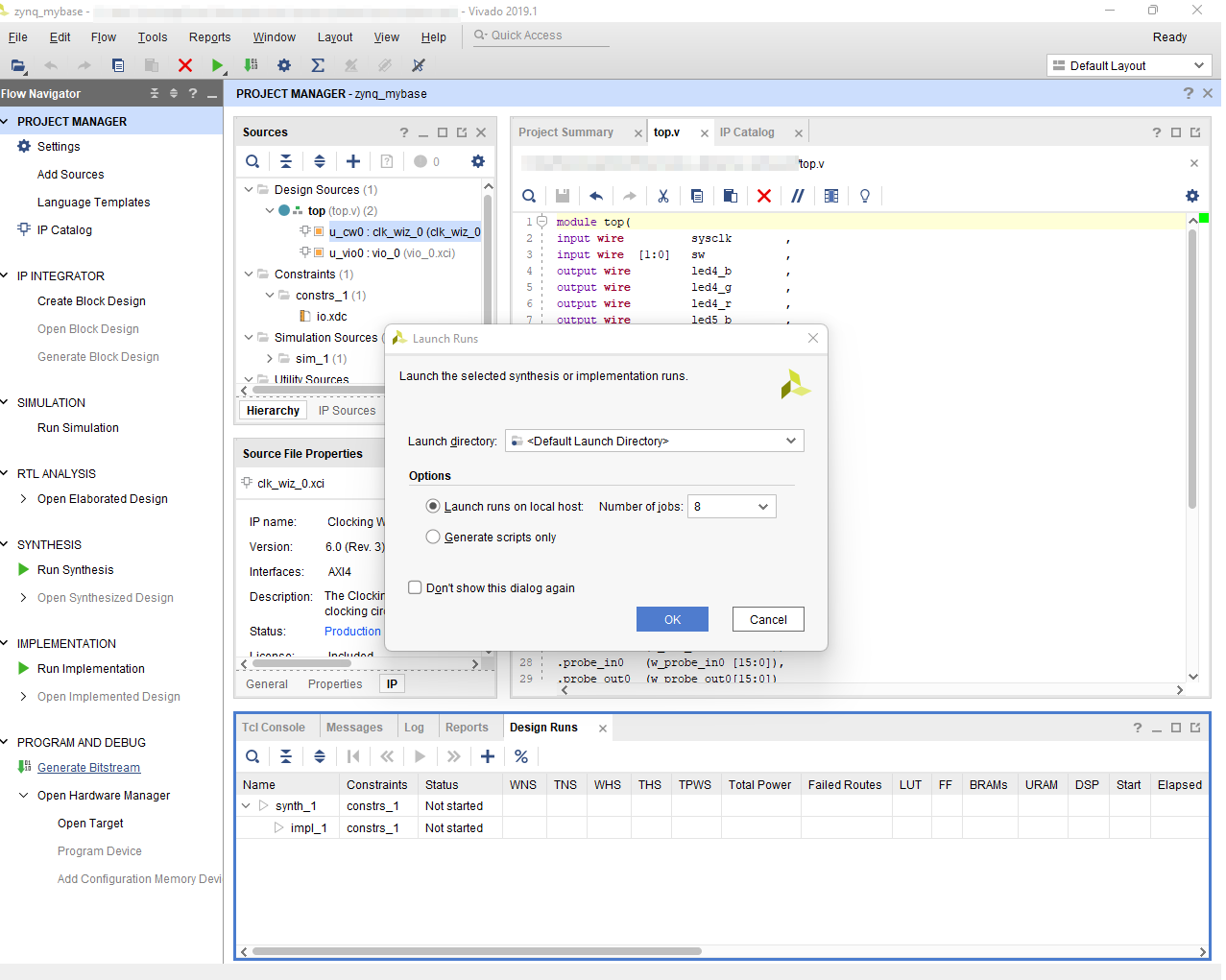
  16. After compilation is finished, its possible to download the design to the pynq-z2.
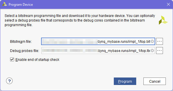
    1. With the board connected to our PC via USB, and powered on, click on Prorgram and debug > Open hardware manager > Open target


    2. Then click program device, and select xc7020_1.


  17. On the program device pop-up, you can select the bitsream and debug probes file. Most times it will automatically load the last compiled bitfile, with its matching debug probes file. Probes file needs to match the debugging logic in the bitfile being downloaded, otherwise it wont be able to connect. If any part of the debugging logic has a design error (missing connections, unmet timing), the debug probes file might not be generated, and it would not be possible to access debugging logic this way.


  18. Go to the hw_vio_1 and add all ports.


  19. Set all output ports bits o be controlled as toggle buttons


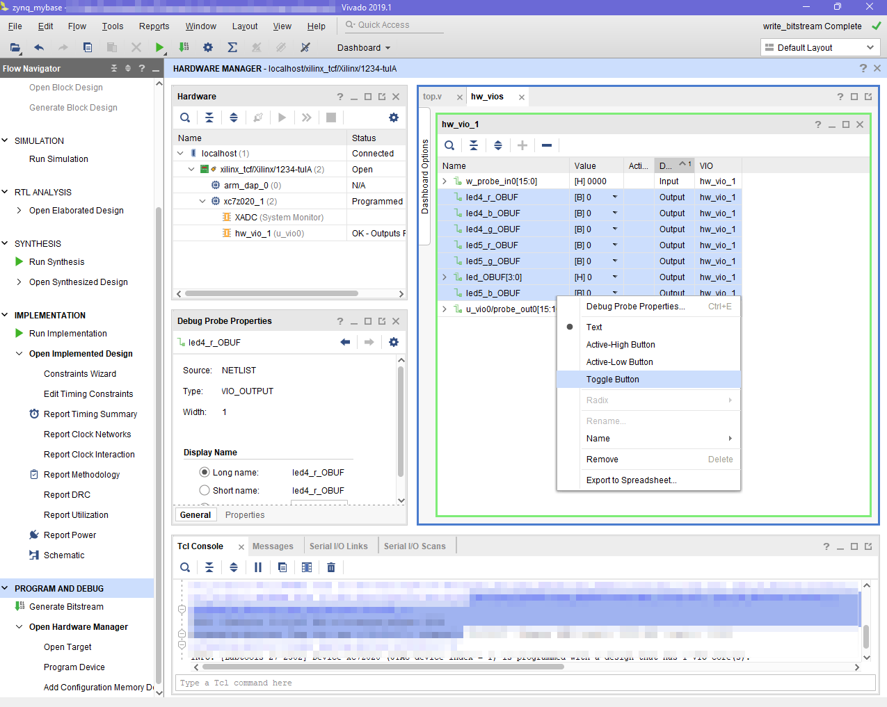
  20. Finally, test pressing some buttons/switches onboard, and see how the input probes change Also toggle some buttons on the VIO to control the onboard leds.


Enjoy!


Attachments:
Download this file (zynq_mybase_src.zip)zynq_mybase_src.zip[ ]2 kB
  Written By Peter Gomez Este contenido esta orientado a los programadores que tienen problema con la conectividad("SGC PmmC") de su pantalla uOled-128-g1/g2…
Written by Sherneyko Plata Rangel   Pynq-z2: Hello world   In this tutorial we will implement a simple test of the inputs/outputs available on…
Objetivos Requerimientos Procedimiento Descripción de Hardware. Qsys. Nios II. UCOS II. Secuencia de Sprite. Sintesis de Audio. Descargas Glosario Otros Resultados. Ejemplo de Sprites.     Objetivos: Diseñar una plantilla general para el diseño de…
Written by Holguer A. Becerra           Requerimientos: DE0-NANO USB-UART(solo para parte 3) Python 2.7 ó superior.   Objetivos: Dar una introducción a los conceptos de Multitasking, Scheduling y…
Written by Holguer A. Becerra             Based on Gregory Estrade's Work.   I have ported the PC Engine System on the DE0-NANO back in 2014, why…
      Arduino tools are generally nice tools for quick prototyping and improvized projects, and the Seeeduino Xiao…
Written by: Holguer A Becerra         En esta practica vamos a construir nuestro primer juego retro  usando un sincronizador de Video VGA…
Written by: Andrea Paola Pabón Ortega & Daniel Enrique Mejia Rueda Revision by: Ing Holguer A. Becerra   DESCRIPCIÓN DEL PROYECTO: El  RTAWD DE0NANO…
  Written by Holguer Andres   Requires: DE0-NANO. 4.3 Inch 480x272 Screen.( WQVGA ) ?️       Parte HW: Descargue la siguiente plantilla( DE0_NANO_TFT_PSP.zip) y descomprimala en una ruta sin espacios y…
Escrito por Guillermo Acevedo   Diseño   En esta practica desarrollaremos un filtro FIR en hardware, para este caso en especifico, realizaremos un filtro…
 Written By Juan David Delgado   FILTRO FIR (FILTRO DE RESPUESTA FINITA AL IMPULSO)     Son conocidos como filtros digitales no recursivos debido a…
XISCKER: Reduced and Complex Instruction Set Computing Key Educational Resources A Configurable Platform for the Emulation of Different Computer Architectures An introduction to Computer Architectures through digital design description for FPGA devices   Computer Architecture embraces all three…
Escrito por: Alix Angarita   En el manual a continuación se explica un método de debug adicional que es muy interesante debido a…
By: Fabio Hernández   INTRODUCCIÓN:   El presente documento pretende mostrar la manera de generar software para una imagen de Linux implementada en la…
Summary Written by Fabio Hernandez   HARD PROCESSOR SYSTEM (HPS)     ------------------------------------------------------------------------------------------------------------------------------------------------   Introducción   Tenemos  2 nuclos de procesamiento ARM cortex-A9, cada uno son su propio cache  se…
Escrito por Jesus Lopez         INTRODUCCIÓN   El acceso directo a memoria (DMA, del inglés direct memory access) permite a cierto tipo de componentes de una computadora acceder a…
    Written by  Sebastian Baquero       Objetivos  Introducción a los conceptos de Multitasking, Scheduling y Context Switching.  Ampliación de los conceptos a cerca de el…