This manual was originally written in the Year 2014 by the Lecturer Holguer A. Becerra for the FPGA course of UPB 31289, and now republished and revised for FPGAlover by the same author.
Quartus Project:
LVDS Pinout of DE0-NANO(Download):
| LVDS GPIOs on DE0-NANO |
|
|
|
| GPIO |
FPGA |
LVDS(P/N) |
JP[N](PIN) |
BANK |
LVDS mode |
F_HSCLK Receiver(MHz) |
F_HSCLK Transmitter(MHz) |
HSIODR Mbps |
| GPIO_1_[1] |
PIN_T15 |
N |
4 |
4 |
LVDS_E_3R |
- |
320 |
640 |
| GPIO_1_[2] |
PIN_T14 |
P |
5 |
4 |
LVDS_E_3R |
- |
320 |
640 |
| GPIO_1_[3] |
PIN_T13 |
N |
6 |
4 |
LVDS_E_3R |
- |
320 |
640 |
| GPIO_1_[4] |
PIN_R13 |
P |
7 |
4 |
LVDS_E_3R |
- |
320 |
640 |
| GPIO_1_[5] |
PIN_T12 |
N |
8 |
4 |
LVDS_E_3R |
- |
320 |
640 |
| GPIO_1_[6] |
PIN_R12 |
P |
9 |
4 |
LVDS_E_3R |
- |
320 |
640 |
| GPIO_1_[7] |
PIN_T11 |
N |
10 |
4 |
LVDS_E_3R |
- |
320 |
640 |
| GPIO_1_[9] |
PIN_R11 |
P |
14 |
4 |
LVDS_E_3R |
- |
320 |
640 |
| GPIO_1_[16] |
PIN_L16 |
N |
21 |
5 |
TRUE LVDS/LVDS_E_3R |
420/- |
420/320 |
840/640 |
| GPIO_1_[19] |
PIN_L15 |
P |
24 |
5 |
TRUE LVDS/LVDS_E_3R |
420/- |
420/320 |
840/640 |
| GPIO_1_[17] |
PIN_K16 |
N |
22 |
5 |
TRUE LVDS/LVDS_E_3R |
420/- |
420/320 |
840/640 |
| GPIO_1_[31] |
PIN_K15 |
P |
38 |
5 |
TRUE LVDS/LVDS_E_3R |
420/- |
420/320 |
840/640 |
| GPIO_1_[18] |
PIN_R16 |
P |
23 |
5 |
TRUE LVDS/LVDS_E_3R |
420/- |
420/320 |
840/640 |
| GPIO_1_[21] |
PIN_P16 |
N |
26 |
5 |
TRUE LVDS/LVDS_E_3R |
420/- |
420/320 |
840/640 |
| GPIO_1_[22] |
PIN_R14 |
N |
27 |
4 |
LVDS_E_3R |
- |
320 |
640 |
| GPIO_1_[25] |
PIN_P14 |
P |
32 |
4 |
LVDS_E_3R |
- |
320 |
640 |
| GPIO_1_[23] |
PIN_N16 |
N |
28 |
5 |
TRUE LVDS/LVDS_E_3R |
420/- |
420/320 |
840/640 |
| GPIO_1_[24] |
PIN_N15 |
P |
31 |
5 |
TRUE LVDS/LVDS_E_3R |
420/- |
420/320 |
840/640 |
| |
|
|
|
|
|
|
|
|
| |
|
|
|
|
|
|
|
|
| GPIO_0_[0] |
PIN_D3 |
P |
2 |
8 |
LVDS_E_3R |
- |
320 |
640 |
| GPIO_0_[1] |
PIN_C3 |
N |
4 |
8 |
LVDS_E_3R |
- |
320 |
640 |
| GPIO_0_[2] |
PIN_A2 |
N |
5 |
8 |
LVDS_E_3R |
- |
320 |
640 |
| GPIO_0_[3] |
PIN_A3 |
P |
6 |
8 |
LVDS_E_3R |
- |
320 |
640 |
| GPIO_0_[5] |
PIN_B4 |
P |
8 |
8 |
LVDS_E_3R |
- |
320 |
640 |
| GPIO_0_[6] |
PIN_A4 |
N |
9 |
8 |
LVDS_E_3R |
- |
320 |
640 |
| GPIO_0_[7] |
PIN_B5 |
P |
10 |
8 |
LVDS_E_3R |
- |
320 |
640 |
| GPIO_0_[8] |
PIN_A5 |
N |
13 |
8 |
LVDS_E_3R |
- |
320 |
640 |
| GPIO_0_[10] |
PIN_B6 |
P |
15 |
8 |
LVDS_E_3R |
- |
320 |
640 |
| GPIO_0_[11] |
PIN_A6 |
N |
16 |
8 |
LVDS_E_3R |
- |
320 |
640 |
| GPIO_0_[12] |
PIN_B7 |
P |
17 |
8 |
LVDS_E_3R |
- |
320 |
640 |
| GPIO_0_[14] |
PIN_A7 |
N |
19 |
8 |
LVDS_E_3R |
- |
320 |
640 |
| GPIO_0_[20] |
PIN_E8 |
N |
25 |
8 |
LVDS_E_3R |
- |
320 |
640 |
| GPIO_0_[21] |
PIN_F8 |
P |
26 |
8 |
LVDS_E_3R |
- |
320 |
640 |
| GPIO_0_[24] |
PIN_C9 |
N |
31 |
7 |
LVDS_E_3R |
- |
320 |
640 |
| GPIO_0_[25] |
PIN_D9 |
P |
32 |
7 |
LVDS_E_3R |
- |
320 |
640 |
| GPIO_0_[30] |
PIN_A12 |
N |
37 |
7 |
LVDS_E_3R |
- |
320 |
640 |
| GPIO_0_[33] |
PIN_B12 |
P |
40 |
7 |
LVDS_E_3R |
- |
320 |
640 |
| GPIO_0_[31] |
PIN_D11 |
N |
38 |
7 |
LVDS_E_3R |
- |
320 |
640 |
| GPIO_0_[32] |
PIN_D12 |
P |
39 |
7 |
LVDS_E_3R |
- |
320 |
640 |
| |
|
|
|
|
|
|
|
|
| GPIO_2_[2] |
PIN_C14 |
N |
7 |
7 |
LVDS_E_3R |
- |
320 |
640 |
| GPIO_2_[7] |
PIN_D14 |
P |
12 |
7 |
LVDS_E_3R |
- |
320 |
640 |
| GPIO_2_[3] |
PIN_C16 |
N |
8 |
6 |
TRUE LVDS/LVDS_E_3R |
420/- |
420/320 |
840/640 |
| GPIO_2_[4] |
PIN_C15 |
P |
9 |
6 |
TRUE LVDS/LVDS_E_3R |
420/- |
420/320 |
840/640 |
| GPIO_2_[8] |
PIN_F15 |
P |
13 |
6 |
TRUE LVDS/LVDS_E_3R |
420/- |
420/320 |
840/640 |
| GPIO_2_[9] |
PIN_F16 |
N |
14 |
6 |
TRUE LVDS/LVDS_E_3R |
420/- |
420/320 |
840/640 |
| GPIO_2_[11] |
PIN_G16 |
N |
16 |
6 |
TRUE LVDS/LVDS_E_3R |
420/- |
420/320 |
840/640 |
| GPIO_2_[12] |
PIN_G15 |
P |
17 |
6 |
TRUE LVDS/LVDS_E_3R |
420/- |
420/320 |
840/640 |


Results:
1. Obtain an HDMI cable and cut one end of it (These cut cable ends will be connected to the LVDS to TMDS translator).
2. Download the template and review where the LVDS channels are assigned(See .QSF) so that you can connect them to the LVDS to TMDS translator.
3. Once you have set up the external scheme for the FPGA, generate the .sof file, connect the HDMI cable to the display, and program the FPGA.
4. What appears on the screen? What resolution and frequency is it displaying? (You should see what is on the video results)
5. On line 46 of the template, modify the parameters, regenerate the .sof file, and verify each of the resolutions.

Relevant Documents
- LVDS Owner’s Manual
- Video Connectivity Using TMDS I/O in Spartan-3A FPGAs
- Implementing a TMDS Video Interface in the Spartan-6 FPGA
- Double Data Rate I/O (ALTDDIO_IN, ALTDDIO_OUT, and ALTDDIO_BIDIR) Megafunctions
- KYANITE Schematic
- VESA TIMINGS
- Support HDMI 1.3 12-Bit Deep Color With the TMDS341A
Explanation
In this practice, we will understand HDMI (High Definition Multimedia Interface) video interface built for the DE0-NANO. To do this, we must understand how TMDS (Transition Minimized Differential Signaling) transmission works and develop a Verilog HDL transmission module capable of controlling this type of video interface using the DE0-NANO (Cyclone IV).
TMDS, or Transition Minimized Differential Signaling, shares similarities with LVDS (Low Voltage Differential Signaling). Both standards involve differential signaling for the input and output of HDMI connectors. However, they differ in terms of voltage parameters and operating ranges, including VIH (High-level input voltage), VIL (Low-level input voltage), VOH (High-level output voltage), and VOL (Low-level output voltage). It's important to note that TMDS is more closely related to Current Mode Logic (CML).", as seen in the following figure.


As shown in the figure, LVDS varies with voltage ranges between 1 and 1.4 V, with a swing of +-350mV and maximum transmission speeds of up to 3.125 Gbps, while CML transmission supports speeds of up to 10 Gbps with operating voltages ranging between 2.7V and 3.4 V and a swing of +-800mV. The following table illustrates the differences between LVDS and CML in terms of their configuration for reception and transmission, information you can read in the "LVDS Owner's Manual" by Texas Instruments.

Similar to CML, TMDS transmission has 50 Ohm pull-up resistors in its receivers and transmitters. Its input and output voltage parameters are also similar, as shown in the table below, which displays the operating ranges of TMDS and the conceptual scheme.


Why is it important to understand TMDS and its differences compared to LVDS?
Altera's Cyclone IV FPGAs do not yet have standards for handling TMDS-type signals. However, this doesn't mean that you can't design an HDMI transmission system. In this case, the Cyclone IV FPGA has LVDS differential channels that can be adapted to TMDS with either AC or DC coupling, as explained in the manual "Interfacing LVDS with other differential I/O types."
What does an HDMI transmitter look like?
An HDMI TX consists of 4 TMDS channels:
Channel 0: It is responsible for transmitting the blue video component and the VSYNC and HSYNC synchronization pulses, similar to what we saw in the VGA practice.
Channel 1: It is responsible for transmitting the green video component and some control commands and encoded audio.
Channel 2: It is responsible for transmitting the red video component and some control commands and encoded audio.
Clock channel: It is responsible for sending the base clock, which VSYNC and HSYNC rely on.
Note: All channels are encoded using the TMDS algorithm, which converts 8-bit video signals per color component into 10-bit encoded signals. The ninth bit is produced through something called "Transition Minimizing," and the tenth bit is produced to maintain an appropriate DC balance in relation to the number of zeros and ones generated after adding the ninth bit.


After the encoding stage of each channel, data serialization follows, where 10 bits must be transmitted per channel. These 10 bits can represent a video pixel, header, or audio sent through the TMDS channels, as shown in the following figure.

HDMI is composed of three TMDS operating modes:
- Video Data Period: When visible video is transmitted.
- Data Island Period: When video is not visible and is used to transmit audio and auxiliary data.
- Control Period: During this period, the necessary headers for transmitting audio and video are sent.

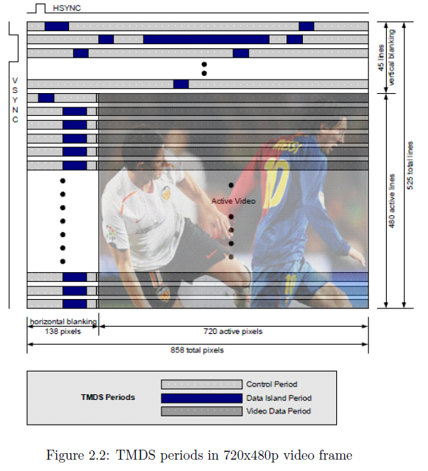


The TMDS clock signal is the pixel_clock signal generated in the original video synchronizer. Each of the 10 bits must be serialized within the period of this signal. This means that the serialization stage must operate with a clock 10 times faster than the pixel_clock.
For example:
- To send a 800x600@60Hz SVGA video signal, assuming the pixel_clock is 40MHz, a clock of 400MHz would be needed to serialize the data properly.
- To send a 1280x720@60Hz 720p video signal, assuming the pixel_clock is 74.25MHz, a clock of 742.5MHz would be required to serialize the data.
Note: The Cyclone IV in the DE0-NANO can generate signals up to 475MHz with its internal PLLs. However, this doesn't mean that you can't create an HDTV video interface for 720p or 1080i. There are other techniques, such as using DDIOs to generate double data rates, to achieve data transmission frequencies of up to 840Mbps using the Cyclone IV's LVDS channels.

In the following image designed by Xilinx Corp (modern FPGAs from this brand are compatible with TMDS standards and don't require coupling), you can observe an HDMI transmitter more closely. In the blue box, you can see the encoding stage, in the red box, the data synchronization stage, in the green box, the signal stage based on the original video clock signal, in the magenta box, the data serialization stage, and in the cyan box, the TMDS differential channels.

Just like when building the VGA synchronizer, the first thing we need to know is the HDMI connector, where:
- Pins 1 and 3 are the channel 2 signals in TMDS.
- Pins 7 and 9 are the channel 0 signals in TMDS.
- Pins 4 and 6 are the channel 1 signals in TMDS.
- Pins 10 and 12 are the clock channel signals in TMDS.
- Pin 13 is the CEC (Consumer Electronics Control) used for sending control commands between devices.
- Pins 15 and 16 are dedicated to DDC (Display Data Channel), used for EDID (Extended Display Identification Channel) communications that use the i2C protocol for information exchange between peripherals.
- Pin 18 is an output that supplies low current at 5V.
- Pin 19 is an input for detecting HDMI cable connection or disconnection.
In the following image, you can observe various boxes. The main box contains the description of the hardware that the Cyclone IV in the DE0-NANO will use for HDMI TX. External to the FPGA, there is additional hardware required to translate LVDS to TMDS, necessary to make LVDS mode compatible with HDMI's native TMDS.


The design within the Cyclone IV(DE0-NANO) includes:
- Video Sync: Responsible for generating signals relative to video activation signals with their respective timing.
- PLL: Responsible for generating the clock signal, maintaining phase, one controlling the video synchronizer, and another multiplying the reference signal of the video synchronizer PCLK (Pixel Clock Reference) by x5. All clock signals go to the FPGA's global clocks.
- TMDS encoder: Encodes RGB, VSYNC, HSYNC, VDE, AUX, and ADE signals.
- LVDS DRIVER: True LVDS I/O mode in the Cyclone IV.
- DDIO: Double Data rate, responsible for sending data outputs at double the necessary frequency (see more).
- Synchronizer: Data synchronizer between low-frequency and high-frequency clocks.
- Serializer: 10:2 data serializer, serializing a bus of 10 bits two by two to send them to the DDIO, which is responsible for sending the data at double the speed in Mbps.
You will have as a foundation the Video Sync, the PLLs, the TMDS encoder, the DDIO, and a small serializer;

you should assemble circuit converter that appears in the image

Note: According to the LVDS Owner's Reference Manual from Texas Instruments, most CML/TMDS receivers have AC coupling at the input, which allows an LVDS output to be connected directly to HDMI inputs without the need for the previous circuit. So good news!, do it under your own risk, FPGAlover does not take any responsibility if you burn or damage your FPGA.
