This DAC(MCP4821) module was developed by the UPB students Jose Velandia & Henry Lizaro in the year 2012 to control the single channel 12-bit Digital-to-Analog converter (DAC) with internal voltage reference of Microchip MCP4821. You will find here the description of the module, plus a very useful application on digital modulations(ASK, FSK, BPSK, QPSK), that you could use to learn more about digital modulations and to visualize at the output of the MCP4821 DAC.

Verilog Module
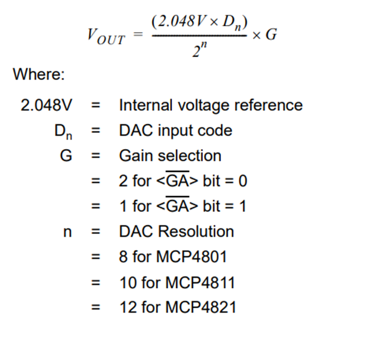
Datasheet of the DAC MCP4821
Instantiation
/*MCP4821*/
MCP4821 Dac_FSM_inst
(
	.clk_40mhz(clk_40Mhz) ,	// input  CLOCK_IN_sig
	.START(start_signal) ,	// input  START_sig
	.TRAMA({~data[11],data[10:0]}) ,	// input [11:0] TRAMA_sig
	.ENABLE(1'd1) ,	// input  ENABLE_sig
	.GAINx2(1'd0) ,	// input  GAINx2_sig
	.SHDN(1'd0), 	// input  HZ_sig
	.CSn(GPIO[0]) ,	// output  CSn_sig
	.SCK(GPIO[1]) ,	// output  SCK_sig
	.SDI(GPIO[2]) ,	// output  SDI_sig
	.LDAC(GPIO[3])	// output  LDAC_sig
);
Module Description:
- This module operates at a clock frequency of 40 MHz.
- It interfaces with an MCP4821 Digital-to-Analog Converter (DAC) and manages the SPI communication protocol.
- The module accepts the following inputs:
START (1 bit): Initiates the Finite State Machine (FSM).TRAMA (12 bits): Data input for the DAC.ENABLE (1 bit): Enables the module.GAINx2 (1 bit): Selects the gain of the DAC (0 for 1x, 1 for 2x).SHDN (1 bit): Controls the shutdown mode of the DAC.
- It has the following SPI interface signals:
CSn (1 bit): Chip Select.SCK (1 bit): Serial Clock.SDI (1 bit): Serial Data Input.
- The module provides one output:
LDAC (1 bit): This signal is used to synchronize and transfer data from the input latch register to the DAC register (output latches, VOUT).
Finite State Machine (FSM) Operation: The module employs a Finite State Machine (FSM) to control the DAC MCP4821 and ensure proper timing and synchronization during the SPI communication. Here's how it works:
-
Initialization (ESTADO_1):
- The module waits for the
START signal to initiate an operation.
-
Data Transfer Setup (ESTADO_2 - ESTADO_4):
- If
START is high, the module proceeds to ESTADO_2, where it checks the other control signals.
- It prepares for data transfer in ESTADO_3 by enabling
SDI_ON.
- In ESTADO_4, data transfer commences, and the module shifts the 12-bit data onto the
SDI line according to the SPI protocol.
-
LDAC Control (ESTADO_5 - ESTADO_6):
- After data transfer, the module manages LDAC synchronization:
- In ESTADO_5, it raises
LDAC.
- After a delay (controlled by
LDAC_ON_H), it transitions to ESTADO_6, lowering LDAC.
-
Idle Period (ESTADO_7):
- In ESTADO_6, it waits for an idle period before starting a new operation.
- This ensures that all signals are in the correct state before initiating another operation.
-
Finish (ESTADO_1):
- After the idle period, the module returns to ESTADO_1, ready for a new operation.
Operation Overview:
- The module's operation is initiated by setting
START.
- It follows the SPI protocol, managing CSn, SCK, and SDI for data transfer.
- LDAC synchronization ensures proper updates to the DAC output.
- The
LDAC signal is used for synchronization and is set as per the timing requirements of the MCP4821 DAC.
- The FSM allows for proper timing and synchronization for DAC operations.
DAC output Calculation for MCP4821

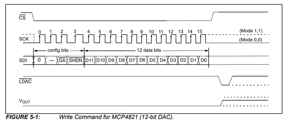
MCP4821 SPI Communication Frame
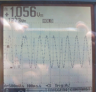
Example on the board DE0-NANO.
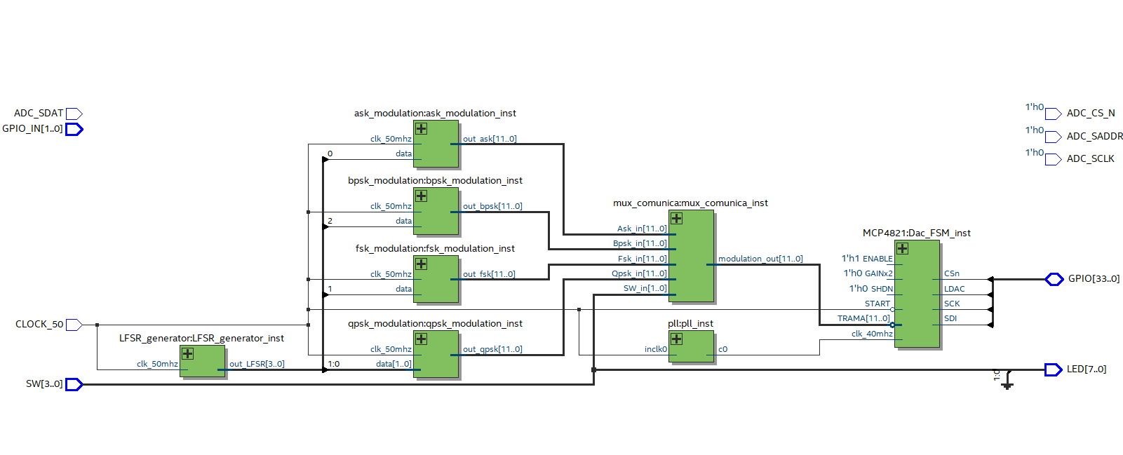
In the following FPGA project example for the DE0-NANO, we have several key components(observe figure below):
-
Random Signal Generator (LFSR_generator): This part creates random data that can be used for various purposes. It runs on a 50 MHz clock and produces 4 bits of random data.
-
Modulation Modules: a. ASK Modulator (ask_modulation): This module takes the random data and uses it to perform Amplitude Shift Keying (ASK) modulation. The result is a 12-bit signal (Ask) that represents information encoded in the signal's amplitude. b. FSK Modulator (fsk_modulation): Similar to ASK, this module employs the clock and random data to carry out Frequency Shift Keying (FSK) modulation. It produces a 12-bit signal (Fsk) with information encoded in the signal's frequency. c. BPSK Modulator (bpsk_modulation): This module applies Binary Phase-Shift Keying (BPSK) modulation using the clock and random data. It generates a 12-bit signal (Bpsk) with information encoded in the signal's phase. d. QPSK Modulator (qpsk_modulation): Using the clock and a 2-bit random data input, this module performs Quadrature Phase-Shift Keying (QPSK) modulation. The output is a 12-bit signal (Qpsk) with information encoded in both amplitude and phase.
-
Multiplexer (mux_comunica): Think of this as a switch. It selects one of the modulation signals (ASK, FSK, BPSK, or QPSK) based on the position of physical switches (SW[1:0]). The chosen modulation signal is then sent to the MCP4821 module.
-
MCP4821 (Dac_FSM_inst): This module connects to the MCP4821 Digital-to-Analog Converter (DAC). It operates on a 40 MHz clock and receives the selected modulation signal. It appears to control the DAC chip and produce an analog signal.
-
GPIO Signals: These signals are used for communication with the MCP4821 chip.
-
LEDs and Switches: The LEDs display information or status, and the switches (SW[1:0]) allow you to select the type of modulation you want to work with. The switch combinations and their corresponding selected modulations are as follows:
- SW[1:0] = 00: ASK Modulation
- SW[1:0] = 01: FSK Modulation
- SW[1:0] = 10: BPSK Modulation
- SW[1:0] = 11: QPSK Modulation
In essence, this project generates various types of modulated signals (ASK, FSK, BPSK, QPSK) using random data. You can select one of these modulated signals using the switches, and the MCP4821 module helps convert this digital signal into analog, which can be used for various applications.
You can download the Quartus project to have a template or to test your MCP4821 DAC
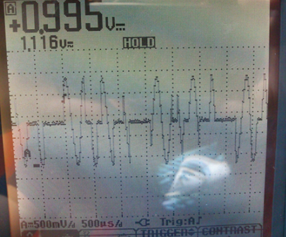
If you synthesize this application example, you need to have a MCP4821 connected to the GPIOs of the FPGA, and then you will see.
- SW[1:0] = 00: ASK Modulation
- SW[1:0] = 01: FSK Modulation

- SW[1:0] = 10: BPSK Modulation
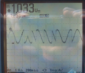
- SW[1:0] = 11: QPSK Modulation