Written by Fabio Andres

In this manual you are going to understand how the SNES Controller Works, and how we can acquire through a simple Finite State Machine (FSM), all the buttons states from the SNES controller using the de0-nano SOC (you can use any FPGA borad, and implement this manual).
It is important to make clear that this manual is based on "SNES timing diagram"(Design Methodology) by Thomas D.
Required Materials:
- Any FPGA board (Though for this manual we are going to use the DE0-NANO-SOC)
- SNES Controller (10 USD on Ebay)
Brief Explanation:
- Let's start by looking at the SNES Controller Pinout:

As you can see The SNES has two gamepad ports which each have 5 wires. Two are the power supply wires: brown (ground) and white (5v). Two of the three remaining wires are used by the SNES to output clock and timing information: yellow (data latch), and orange (data clock) y el Puerto restante es el rojo (DATA).
- The SNES sends a 12 us positive impulse on the data latch wire (yellow). This data latch indicates the SNES will start sending 16 data clock periods to the gamepad on the clock wire (orange) which are used by the gamepads to indicate what buttons are pressed. Each of the 16 data clock periods represent a different button, and the SNES will expect the output signal to toggle on those data clock periods which indicates a button on the gamepad is pressed.
There are 12 buttons on the SNES gamepad, but the SNES sends 16 data clocks periods. Only the first 12 data clock periods are used, the following 4 are ignored by the SNES. The protocol was first designed for the NES console which had less buttons. Nintendo added new buttons on the SNES but didn't change the communication protocol as it could support more buttons. Potentially, this protocol could support up to 16 different buttons.

- Once the logical procedure is understood, the following step is to put this into a FSM Diagram to make it more understandable.

- The previous FSM diagram is composed by 5 different states which are necessary to get the buttons status from SNES controller:
- IDLE: this state set up the delay in 12 microseconds and, if the signal start is high, go to the next state.
- STATE1: in this state the LATCH signal is high, and stay in this status as long as the delay is greater than zero, when have passed 12 microseconds, the FSM go to the next state.
- STATE2: in this state the LATCH signal goes from high state to low state and the clock signal hold in high state as long as the delay is greater than zero, when have passed 6 microseconds, the FSM go to the next state.
- STATE3: in this state all the signals hold in low state (the clock signal goes from high state to low state) From now on whenever a flank is down it takes a button and it is stored in the buttons_temp vector [14: 0] (always@ negedge clk_snes) if the module have saved all the 16 buttons state, the FSM go to the next state, else , the FSM returns to the state 2 and save a new botton state.
- STATE4: in this state the clock signal hold in high state as long as the delay is greather than zero, when have passed 12 microseconds the FSM go to the next state.
- FINISH: in this state the finish signal hold in high state and the bottons state are sent to the output of the module and the FSM goes to the IDLE state.
- The above description can be represented by the following graph through time:

- Now it is time to see the Verilog Code, for this logic.
- Verilog Module pinout:
module SNES_FSM( input clk_50, input start, input data_in_snes, output reg [11:0]buttons_snes, output finish, output idle, output latch_snes, output clk_snes ); - States and control signal declaration:
//LATCH______CLOCK_____FINISH____IDLE______STATE localparam IDLE = 10'b0_____________1_________0________1______000001; localparam STATE1= 10'b1_____________1_________0________0______000010; localparam STATE2= 10'b0_____________1_________0________0______000100; localparam STATE3= 10'b0_____________0_________0________0______001000; localparam STATE4= 10'b0_____________1_________0________0______010000; localparam FINISH= 10'b0_____________1_________1________0______100000; //numero de clocks del relog base de 50 Mhz localparam TIME6u = 10'd300; localparam TIME12u = 10'd600; reg [9:0]state=IDLE; reg [9:0]delay=TIME12u; reg [3:0]num_clks=4'd0; reg [14:0]buttons_temp=15'd0; wire pre_finish=(state[9:0]==STATE4)?1'b1:0; assign latch_snes=state[9]; assign clk_snes=state[8]; assign finish=state[7]; assign idle=state[6]; - Main FSM:
always@(posedge clk_50) begin case(state[9:0]) IDLE :begin state[9:0]<=IDLE; delay[9:0]<=TIME12u; num_clks[3:0]<=4'd0; if(start==1) begin state[9:0]<=STATE1; end end STATE1:begin state[9:0]<=STATE1; delay[9:0]<=delay[9:0]-1'b1; num_clks[3:0]<=4'd1; if(delay[9:0]==10'd0) begin delay[9:0]<=TIME6u; state[9:0]<=STATE2; end end STATE2:begin state[9:0]<=STATE2; delay[9:0]<=delay[9:0]-1'b1; num_clks[3:0]<=num_clks[3:0]; if(delay[9:0]==10'd0) begin delay[9:0]<=TIME6u; state[9:0]<=STATE3; end end STATE3:begin state[9:0]<=STATE3; delay[9:0]<=delay[9:0]-1'b1; num_clks[3:0]<=num_clks[3:0]; if(delay[9:0]==10'd0) begin num_clks[3:0]<=num_clks[3:0]+1'b1; if(num_clks[3:0]<4'd15) begin delay[9:0]<=TIME6u; state[9:0]<=STATE2; end else begin delay[9:0]<=TIME12u; state[9:0]<=STATE4; end end end STATE4:begin state[9:0]<=STATE4; delay[9:0]<d=delay[9:0]-1'b1; num_clks[3:0]<=4'd0; if(delay[9:0]==10'd0) begin state[9:0]<=FINISH; end end FINISH:begin state[9:0]<=IDLE; delay[9:0]<=10'd0; num_clks[3:0]<=4'd0; end default:begin state[9:0]<=IDLE; delay[9:0]<=10'd0; num_clks[3:0]<=4'd0; end endcase end - shift register to save button states:
always@(negedge clk_snes) begin buttons_temp[14:0]<={data_in_snes,buttons_temp[14:1]}; end - When FSM has acquired all the buttons, sends them to the output of the module:
always@(posedge pre_finish)
begin
	buttons_snes[11:0]<=buttons_temp[11:0];
end
- Verilog Module pinout:
- Once we have taken a look at the FSM diagram and the Verilog description, we can simulate using ModelSim to verify that the designed FSM works properly, and we meet the timing specifications.

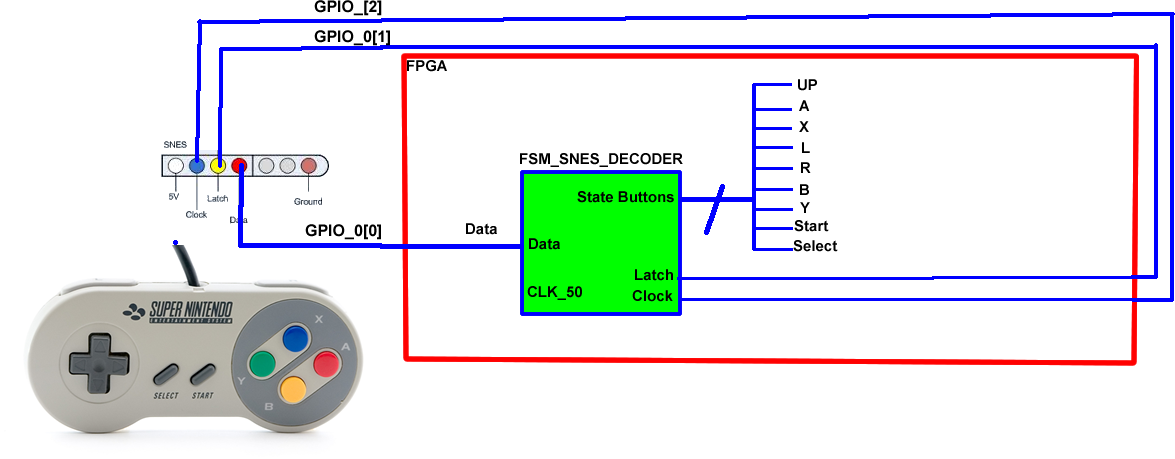
- Finally, after designing and simulating, we are ready to implement the module using any FPGA board, for this example, the DE0-NANO-SOC is used to conduct the experiment.
- Here the necessary verilog modules to use the SNES controller module:
- Here the complete template, and running example using the de0nano
- ENJOY!